Original Link: https://www.anandtech.com/show/1094
Intel 875P (Canterwood) Chipset - The New Flagship
by Anand Lal Shimpi on April 14, 2003 6:37 AM EST- Posted in
- CPUs
We've been paitiently awaiting the arrival of Intel's dual-channel DDR chipsets ever since we first heard the names Springdale and Canterwood almost a year ago at Computex in Taipei. And although the launch of the mainstream Springdale chipset (865) is still a few weeks away, we're finally able to tell you all there is to know about the successor to the aging 850E chipset; what was once known as Canterwood, is now publicly available as the Intel 875P chipset.
The 875P chipset marks a few milestones for Intel; for starters, it depicts Intel as a company that does listen to the needs and requests of their customers - mainly in its support for DDR400 memory technology. Embracing DDR400 SDRAM is something we never thought we would see Intel do, especially considering their stance on the technology in the past, thus we were quite surprised when we heard of the possibility last year at Computex.
The Intel that is today releasing the 875P is very different from the Intel that we remembered forcing Rambus DRAM on the market in the days of the 820 chipset. The Taiwanese motherboard manufacturers couldn't be happier that they finally have chipsets from Intel that are high in demand; it was quite an ordeal for them when Intel was forcing chipsets down their throats that no customer wanted to touch with a ten foot pole.
The next milestone that's set with the 875P is that Intel has finally released a chipset to push RDRAM out of their product lineup; not that there's anything wrong with RDRAM these days, but the fact of the matter is that DDR is far more plentiful and thus much more attractive to end-users and resellers.
Then we actually get to the extensive feature list of the 875P; 800MHz FSB, dual channel DDR400, a new bus made specifically for Gigabit Ethernet, and native Serial ATA with RAID functionality top off what you can expect from the new chipset. With that said, there's quite a bit to mention so we'll spare you the small talk and get right down to it…
The 800MHz FSB is Here
Originally the 800MHz FSB was planned only for Prescott, the upcoming 90nm Pentium 4 core, but with Intel running into thermal and manufacturing walls with their current 0.13-micron process they needed another method of keeping performance competitive without resorting to increasing clock speeds.
We've already described, in great detail, the benefits of moving to an 800MHz FSB in our Sneak Peek article as well as our review of the first 800MHz FSB CPU - the Pentium 4 3.0C. The 875P chipset is the first new chipset from Intel to offer official support for the 800MHz FSB frequency; seeing as how the chipset is positioned as the flagship solution for the Pentium 4 it's no surprise that it's being launched alongside the 3.0C, the flagship 800MHz FSB processor.
|
Enabling 800MHz FSB support on the 875P chipset itself was more of a validation task for Intel; in fact, the amount of work Intel had to do in order to enable the support was relatively minimal considering that many 845PE chipsets will work fine at the increased frequency. Intel will not be offering 845PE chipsets with official support for the 800MHz FSB, so approach such boards at your own risk.
One thing to keep in mind about the 875P chipset is that it will not work with 400MHz FSB CPUs, only 800/533MHz parts. If you want 400MHz FSB support you'll have to wait for the 865/Springdale chipset.
Given that a 64-bit 800MHz FSB offers at most 6.4GB/s of bandwidth between the Memory Controller Hub (MCH aka North Bridge) and the CPU, what sort of memory subsystem does the 875P use to offer balanced bandwidth between the MCH and the memory banks?
DualDDR400 - Intel Follows NVIDIA's Lead for Once
NVIDIA was the first to tout the benefits of a dual channel DDR memory architecture on the desktop with their nForce chipset, announced almost two years ago. With nForce2, NVIDIA finally had a success on their hands and began taking advantage of the added memory bandwidth offered by a dual channel (128-bit) DDR memory interface. Through optimizations of the ball layout and packaging of the nForce2 IGP/SPP (aka North Bridge), NVIDIA helped enable cost effective 4-layer motherboard designs with a 128-bit DDR memory interface, something most nay-sayers claimed was impossible.
Intel followed a very similar methodology with their 875P chipset which, as you can guess by now, also features a dual channel DDR memory interface. By effectively designing the physical interface of the MCH to the motherboard from the outside-in, Intel optimized the MCH for use in cheap 4-layer motherboard designs.
Normally in chipset design, the packaging team worries mostly about internal routing and pays less attention to the routing that motherboard manufacturers will have to do once the chip is in their hands. With the 875P, special attention was paid to the ball layout on the interface side of the MCH to provide for optimal routing. Remember that with a dual channel memory architecture there are twice as many memory interface pins, and for 64-bit DDR channels that makes things quite messy on the motherboard.
This layout optimization is something that is present on the nForce2 and is mainly in place because of the 865 chipset, as that will be a much more cost-sensitive solution than the flagship 875P. Intel is also quite proud of the fact that the 875P's MCH has a package the same size as the 845G, thanks to a smaller manufacturing process.
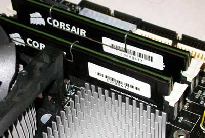
As we mentioned before, the 800MHz FSB offers a maximum of 6.4GB/s of bandwidth between the processor and the MCH; to maintain bandwidth balance, the 875P's dual channel DDR memory controller supports DDR400 which, when installed in pairs offers the same 6.4GB/s of bandwidth as the chipset's FSB.
Dual DDR in action
The MCH is relatively flexible when it comes to basic memory speeds and configurations, but is quite picky when you dive a bit deeper in order to ensure stability and that the chipset meets Intel's rigorous validation standards. What we mean by this is that the 875P can be run in either single channel or dual channel mode, and supports DDR266/333 as well as DDR400 operation. With that said, there are a few very specific requirements for dual channel operation:
- DIMMs must be installed in pairs
- Each DIMM in a pair must be the same size (e.g. 128MB, 256MB, etc…)
- Each DIMM must use the same density memory chips (e.g. 128Mb, 256Mb chips, etc…)
- Each DIMM use the same DRAM bus width (x8 or x16)
- Each DIMM must be either single-sided or dual-sided, you cannot mix a single and a dual sided DIMM in a pair
If any of these stipulations are violated, then Intel specifies that the motherboard should default to single-channel mode, however it is up to the motherboard manufacturer to determine how strictly they wish to enforce this.
The DIMMs in a pair may be different brands, timings and/or speeds, the timings/speeds will be determined by the slowest of the two modules.
Unlike the 865, the 875P MCH supports ECC memory which is one indication (you'll see another later) that the 875P is not only targeted at enthusiasts but also the entry-level workstation market.
One question end-users will be asking themselves is whether the dual channel DDR benefits are worth upgrading to 875P instead of an 845PE motherboard that has been tested to work at the 800MHz FSB. In order to answer this question we looked at the 875P in both single and dual channel memory configurations:
|
Going to a dual channel architecture ends up improving performance between 0 and 15% depending on the application, which isn't insignificant but its worth should be determined by the price difference in motherboards and what the added performance means to you. Also remember that with an 800MHz FSB 845PE motherboard you won't get any of the additional features that come with an 875P solution.
Performance Acceleration Technology
The other aspect of the 875's memory controller that's worth mentioning is what Intel likes to call their Performance Acceleration Technology, or PAT. From the company that came up with terms like Hyper-Threading and NetBurst, you would expect a bit more from the marketing folks instead of "Performance Acceleration Technology" but when are we ever pleased with the marketing guys?
The gist of PAT is that in order to differentiate the 875P from the 865, Intel began speed binning the chipsets and selected the top performing MCHs to be 875P parts with everything else that still qualified ended up being branded as an 865. The benefit of this approach is that Intel can be a bit more aggressive with the memory controller while still ensuring reliable operation. It turns out that these high speed bins are able to shave off, at most, two clocks off every memory access which ends up improving overall performance by a few percent.
Intel's approach to chipset binning is much like the approach they apply to CPU speed binning, which is how they determine what constitutes a 3.0GHz Pentium 4 and a 2.80GHz Pentium 4. With that said, there's no additional logic that must go into enabling PAT, which leads us to believe that in theory, enabling the technology on an 865 motherboard would be possible. Enabling PAT on an 865 would be akin to running a 1.6GHz Pentium 4 at 2.2GHz, meaning that if we were able to enable PAT on an 865 that would be overclocking; whereas PAT on the 875P is a fully validated and supported operating mode. It's not clear whether a motherboard manufacturer would even be able to enable PAT as a BIOS option on 865 chipsets or if Intel has put hardware limitations in place to prevent it from working on anything but the 875P. We'll surely find out in the coming weeks once 865 motherboards are released...
CSA: ooh look, a new Bus
Gigabit Ethernet is slowly but surely becoming the standard that replaces 100Mbit Ethernet on high performance desktops and workstations everywhere. The problem that exists however is that most of these high performance desktops and workstations only have 32-bit 33MHz PCI slots which, if you do the math, ends up being exactly 1Gbps of bandwidth.
Now if you're transferring only in one direction and you have nothing else eating into that 1Gbps of PCI bus bandwidth, then you're not bandwidth limited at all by the PCI bus, but chances are that this perfect world we just described isn't too realistic in your work environment.
Most of the time you're transferring in two directions, and assuming you're connected to a full duplex switch, you're dealing with a peak of 2Gbps of bandwidth. At the same time, you've usually got some disk activity going on in the background among other things that make it clear that 1Gbps of bandwidth isn't going to cut it for some current and most future usage scenarios with Gigabit Ethernet.
Intel saw the bandwidth limitation to current desktop/workstation Gigabit Ethernet deployments and wanted to make their Gigabit solutions more attractive by introducing a new bus to the MCH - the Communications Streaming Architecture (CSA) bus. We're actually giving the bus a little too much credit by calling it new, this is actually a virtually identical copy of a bus that's been present in Intel MCH's for quite some time; the CSA bus is nothing more than a copy of Intel's Hub Link 2.0 bus that connects the MCH to the ICH (aka South Bridge), but instead, this bus is used to connect the MCH to Intel's Gigabit Ethernet controller.
The CSA bus is perfectly matched for Gigabit Ethernet as it offers a total of 2Gbps of bandwidth (266MB/s, equal to that of the Hub Link 2.0 bus because they are two separate but identical links), which is enough for full duplex Gigabit transfers.
 |
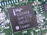 |
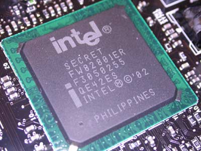
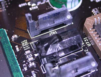
In order to test the usefulness of Intel's CSA we setup a client/server setup composed of one server and two clients all going through a D-Link Gigabit switch using Category-6 cabling. All three systems made use of Intel Gigabit Ethernet controllers; we used Intel Pro/1000 Desktop MT controllers (see top right) in the clients and alternated between another Pro/1000 Desktop controller and the on-board CSA controller (see top left) for the server. Using NetIQ Chariot we generated bidirectional traffic between each client and the server to attempt to saturate the full-duplex Gigabit Ethernet link to the 875P equipped server. Here are the results we came about:
|
As you can see, Intel's CSA does deliver as promised, although you have to keep in mind that transfer rates this high are impossible if you're reading data off of a hard drive. If you're sending data that's already cached in main memory then you'll be able to reach these sorts of transfer rates, otherwise there will be minimal peak transfer rate differences between a CSA Gigabit interface and a conventional PCI Gigabit interface. There's one thing for sure, with a CSA Gigabit interface, your network performance is entirely disk limited.
Even if you're not getting higher transfer rates, moving bandwidth-heavy traffic off of the PCI bus helps to ensure that other transactions occurring on the bus remain uninterrupted by bursts of network traffic. The end result is similar to what NVIDIA was able to achieve using isochronous Hyper Transport channels with nForce2, in that you get uninterrupted network data transfers and minimize the impact of sudden bursts of data on the rest of the system.
The addition of the CSA bus means that the MCH now has the following links stemming from it:
- 32-bit AGP 8x interface
- 2 x 64-bit ECC DDR memory interfaces
- 64-bit NetBurst FSB interface
- 16-bit Hub Link ICH interface
- 16-bit CSA interface
The addition of the CSA bus along with the two 64-bit memory buses are what make the 875P chipset the largest desktop chipset to date with over 1000 balls connecting the MCH to the motherboard.
A New ICH
If you haven't gotten the hint already, Intel went all-out with the 875P and the trend continues with the chipset's new I/O Controller Hub - ICH5.
There are two major features of ICH5 that separate it from its predecessor, ICH4; the first feature is integrated support for a total of 8 USB 2.0 ports. Intel claims that this is the last time they will be upping the number of USB ports supported as 8 seems to meet the current and foreseeable demand.
The next and quite possibly the most important feature of ICH5 is its integrated Serial ATA controller. Current Serial ATA controllers use a PCI interface to the South Bridge (or MCH) and thus eat into the 133MB/s of bandwidth that is allocated to the collection of all 32-bit 33MHz PCI slots on a motherboard. Well, if you look at the Serial ATA specification you'll notice that the maximum transfer rate is listed as 150MB/s, that's 13% more bandwidth than a 32-bit/33MHz PCI bus can provide! Whether or not drives are currently reaching even half of that maximum transfer rate isn't an issue, regardless of what the case is, you never want to create additional bottlenecks; by placing the Serial ATA controller off of the PCI bus, a bottleneck is created that would only be exposed down the road.
Intel's ICH5 gets around this problem by bringing the Serial ATA controller onto the ICH and bypassing the PCI bus all together. The Serial ATA controller has a direct link to the Hub Link 2.0 interface in ICH5 and thus can offer a full 150MB/s per channel. ICH5 features two Serial ATA channels (supporting a maximum of two drives) and two Parallel ATA channels (supporting a maximum of four drives), all of which may be enabled and used concurrently.
Because ICH5 is so new, there is no support for the chip in Intel's Application Accelerator drivers, which is why some I/O intensive benchmarks will show the 875P platform as performing much worse than it should be. Hopefully Intel will remedy this situation as quickly as possible, as it really is quite disappointing to see a brand new platform like the 875P not performing to the best of its potential due to driver limitations.
Promise & HighPoint Say Goodbye to Hollywood - Intel's RAID Arrives
For years now companies like Promise and HighPoint have been offering IDE RAID solutions to motherboard vendors, bringing features like RAID 0, RAID 1 and RAID 0+1 to end users at relatively low price points.
What most users don't understand however is that those IDE RAID controllers featured on most motherboards don't actually handle any processing themselves, they do little more than offer a couple of IDE channels and a BIOS to configure the RAID array - all the processing is done by your CPU. It is actually preferable for your CPU to handle all of this sort of processing simply because a 3GHz Pentium 4 is much faster at these sorts of tasks than a slow dedicated microprocessor would be, not to mention that it's much more cost effective this way.
Given that the CPU was doing the majority of the work to begin with, and RAID had become a common enough technology on motherboards, Intel decided to include Serial ATA RAID functionality in a premium version of their ICH5 known as ICH5R.
The feature set of ICH5R is identical to that of ICH5 but with one exception, RAID 0 support. The ICH5R also has RAID 1 support but that will require a driver/BIOS update in order to enable the support; we're expecting the update within the next month or so. There's nothing too special about Intel's RAID 0 support, but do keep in mind that the RAID only applies to the two Serial ATA channels on the motherboard, not the Parallel ATA channels.
Where Intel is able to offer some additional value over the competition is in their RAID Application Accelerator drivers. Normally when you want to upgrade from a single drive to a dual drive RAID 0 array, you have to backup all of your data and create the RAID 0 array, which ends up destroying all the data you had on the original drive. Intel's solution simply requires you to enable Intel RAID in the BIOS, even when you only have one drive, and upon upgrading to a second drive you simply tell the Application Accelerator driver to create a RAID 0 array and the array is created in the background without any data loss.
The process works quite well and makes upgrading to a RAID 0 setup quite easy; don't let the ease of migration fool you though, moving to a RAID 0 setup actually increases the chance of data loss. With only one drive in a system your data is safe so long as that one drive doesn't fail, but with two drives in RAID 0, should any one of them fail, you could potentially lose all of your data.
Intel's 875P Motherboard
We have a total of six 875P based motherboards in the lab right now and you'll see reviews of them over the next several days, but for this review we used Intel's own D875PBZ.
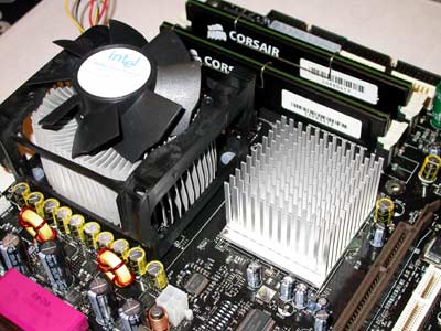
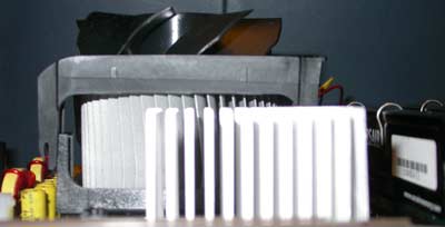
The heatsink on the MCH is almost as tall as the retail Pentium 4 heatsink
The Test
|
Windows
XP Professional Test Bed
|
|
|
Hardware
Configuration
|
|
| CPU |
Intel Pentium 4 3.06GHz
|
| Motherboard |
ABIT
BH7 - Intel 845PE Chipset
Gigabyte SINXP1394 - SiS 655 Chipset Intel D850EMV2 - Intel 850E Chipset Intel D875PBZ - Intel 875P Chipset |
| RAM |
2
x 256MB DDR400 CAS2 Corsair XMS3200 DIMM
2 x 256MB PC800 Samsung RIMMs |
| Sound |
None
|
| Hard Drive |
80GB
Western Digital Special Edition 8MB Cache ATA/100 HDD
|
| Video Cards |
ATI
Radeon 9700 Pro
|
Content Creation & Office Performance
|
|
Here we see the unfortunate effects of not having Intel Application Accelerator support for the new ICH, thus the 875P falls behind even the 845PE; updated drivers will fix this issue.
Gaming Performance
|
|
|
|
|
Video Encoding Performance
|
Professional 3D Performance
|
|
|
|
|
|
Final Words
The 875P has clearly done its job of replacing the long-lived 850/850E at the top of Intel's Pentium 4 chipset line; not only has it done its job, but the 875P does its job quite well.
The beauty of the 875P chipset doesn't lie in its performance, because the performance we see here today we've seen for quite some time courtesy of the 850E chipset; no, the beauty of the 875P lies in its extensive feature set.
The support for dual channel DDR400 and 800MHz FSB are the types of improvements we expect to see with every new chipset generation, but with the 875P the moons just happened to be in proper alignment because we received features such as native Serial ATA support, Intel RAID and a very useful CSA bus for Gigabit Ethernet.
The performance improvement that the 875P offers over the 850E is negligible, assuming you're not transitioning to one of the newer 800MHz FSB CPUs. If you are making the transition to an 800MHz FSB CPU with Hyper Threading support, then the 875P migration makes the most logical sense, however upgrading from an 850E to an 875P with anything other than an 800MHz FSB CPU wouldn't be worth it.
When comparing the 875P to the 845PE, the two are clearly in very different classes, much like the 850E and 845PE were in two very different segments. The upgrade to an 875P from a 845PE platform will result in a somewhat noticeable performance boost, but where you start getting very serious performance gains is when you're talking about upgrading from something older than an 845PE (e.g. original 845, 845 DDR, etc…).
With that said, the 865 chipset may be the one to wait for; the 865 will be noticeably cheaper and only lacks Intel's PAT, which we've yet to come to a consensus on the usefulness of. We're already getting in 865 based motherboards for review, we'll shortly be able to give you all of the information you need to make the appropriate decision between the 875 and the 865. If the 865 performs anything like the 875P then SiS' 655 will almost inevitably be confined to the low-end of the market segment, but in the end the consumer benefits as having an entry-level dual channel DDR Pentium 4 chipset is nothing to complain about.
For now, kudos to Intel on a job well done with their latest line of Pentium 4 chipsets; times have definitely changed since Intel's series of chipset fumbles a couple of years back, and they have changed for the better.
Stay tuned for much more 875P coverage this week as we review the first shipping motherboards out of Taiwan…


